The headline sounds like the obvious thing: of course, if you can make your own CPUs for your projects, then you don’t have to rely on CPU manufacturers. “But wait”, you would ask, “Aren’t CPU design and manufacture very expensive?”
Yes, they are. Wikipedia explains that a project to design a high-end CPU can easily cost US $100 million and require 400 man-years. $100M is a huge sum; it’s a mind-boggling figure. But everything should be put into context:
– Cray Inc. was awarded a US $188 million contract to build Blue Waters;
– Titan cost US $97 million;
– Tianhe-2 cost US $390 million.
Now, the $100M figure doesn’t sound that big, does it? And just for more context: Intel’s revenues in 2012 were US $53341 millions — this is the cost of 533 “typical” CPU design projects.
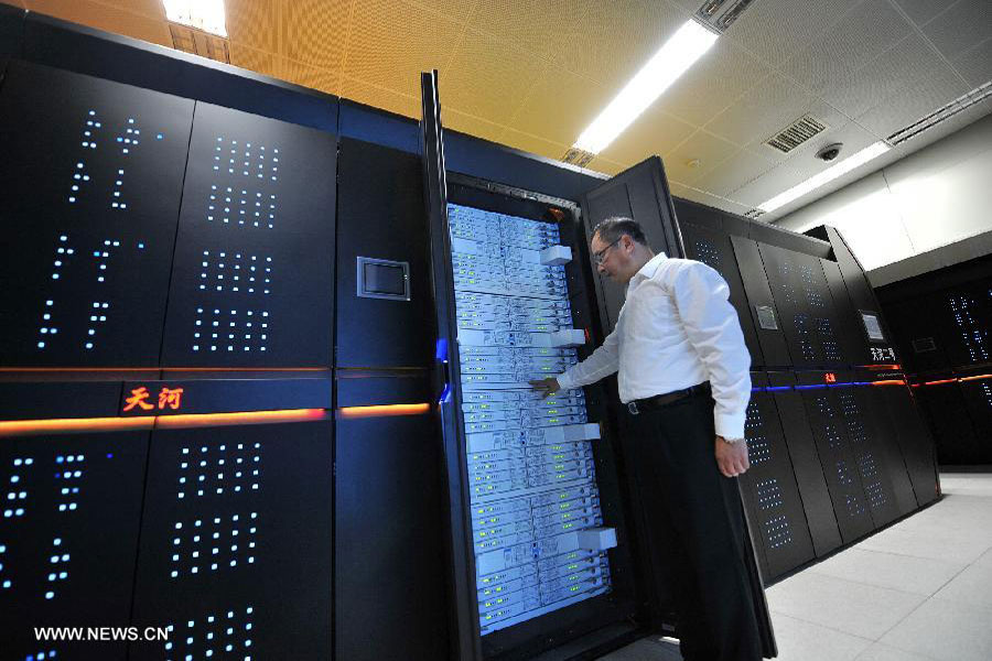
Tianhe-2, the fastest supercomputer in the world as of today, contains 32,000 Intel Ivy Bridge chips and 48,000 Intel Xeon Phi chips. Photo by Xinhua/Long Hongtao, via China Radio International’s English Service.
So it is not really that expensive; but it is difficult to organise, because you need to gather a hundred or two of top-notch engineers from many different fields, put them together, and motivate them for the work that can take many years before first “palpable” results are available.
The good news is that R&D costs of the CPU design project are amortised over large batches of manufactured items: the more items are manufactured, the less is the per-unit R&D cost. For example, the Chinese Tianhe-2 supercomputer pictured above contains 32,000 Intel Ivy Bridge chips and 48,000 Intel Xeon Phi chips, for a total of 80,000 hi-end CPUs. Future exa-scale machines are likely to contain at least 1 million of such chips. If you divide our $100M R&D costs by 1 million items to be manufactured, then it’s just $100 per each CPU. Not much!
There are also manufacturing costs, of course. John L. Hennessy and David A. Patterson give the following estimation in their book “Computer Architecture: A Quantitative Approach” (see page 32):
Processing of a 300 mm (12-inch) diameter wafer in a leading-edge technology cost between $5000 and $6000 in 2010. Assuming a processed wafer cost of $5500, the cost of the 1.00 cm² die would be around $13, but the cost per die of the 2.25 cm² die would be about $51 (…)
How large are today’s CPUs? Intel Xeon E5-2680, such as one used in “SuperMUC”, is implemented in 32 nm technology and is said to have a die size of 435 mm². According to the formula for die count estimation (the same formula is used in the book by Hennessy and Patterson), this gives us roughly 130 dice per a 300 mm wafer. Not all dice are good, so we employ a formula for die yield from page 31 of the book with “typical” parameters, and get a yield of 18%. That is, 23 dice out of 130 are good, and with a wafer processing cost of $6000 this gives a cost of $260 per each good die. (You can make smaller but less capable chips if you wish to increase die count. Note also that dice that contain one or two defects can just have corresponding units, such as cores or cache memory blocks, disabled. This results in a slightly “degraded” but still very usable product, so do not become misguided by the low yield calculated above. See also “Update” at the end of the blog post).
You need to add testing and packaging costs, and also mask set costs, but the manufacturing cost per CPU will probably stay below $500. Add to this R&D costs per unit, which we calculated above at $100, and the grand total becomes $600. For comparison, Intel’s recommended customer price for their Xeon E5-2680 chip is $1723. And you don’t need marketing costs, because you will be the main consumer of your own chips.
This way you can make your own CPUs, suited to your specific HPC requirements. “But wait, there’s more”. You can further encourage people to use your CPUs if they are suitable for other purposes. What about servers? According to IDC, the number of servers shipped in 2012 was 8,1 million units. Wider use of the new CPUs will benefit everyone, urging a boost in operating system and compiler technologies.
But how can you make a CPU that is suitable for both HPC and server workloads? Here comes an interesting part. We propose a hybrid CPU, with multi-core and many-core parts, and the on-chip InfiniBand controller. Various parts of the CPU are used differently depending on the workload (click to enlarge):
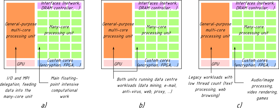
Three use cases for the proposed system with corresponding workloads: (a) HPC environments, (b) generic data centre environments, (c) desktop computing environments
For HPC workloads, the multi-core part is used to feed data to be processed into the many-core part, and also performs delegation of collective MPI communications on behalf of the many-core part. The many-core part serves as the main floating-point engine.
For server workloads, both parts — multi-core and many-core — can execute standard server applications, such as web and e-mail, as well as perform trendy data mining jobs.
You can even use this CPU in desktop computers: the multi-core part will run legacy applications such as word processing and web browsing, while the many-core part will be used to do video rendering for your home theatre and image processing for your graphics editor.
To learn more, read our paper at arXiv:
K.S. Solnushkin, Y. Tsujita, “Marrying Many-core Accelerators and InfiniBand for a New Commodity Processor”
(link: arXiv:1307.0100) (cite with BibTeX)
I also highly recommend the presentation that includes more details.
The work was presented at one of the workshops of the International Conference on Computational Science (ICCS 2013), which was held June 5 — 7, 2013 in Barcelona, Spain. That particular workshop had a prolonged deadline, and the papers didn’t get into the official conference proceedings, so me and my collaborator Dr. Yuichi Tsujita chose to post our paper at arXiv.
To summarise: the coming exa-scale era changes the rules of the game. Designing your own CPUs becomes economically viable. If your country is striving to build an exa-scale supercomputer and expects to spend huge sums of money to buy proprietary components from foreign companies, maybe you should consider investing these money into your own economy and creating your own CPUs.
Update. If you want to increase yield — the fraction of good dies — you can use redundancy. Chip components that are manufactured with defects or get faulty after deployment will be disabled, and the redundant part will be used instead. You can add redundant cache rows or redundant execution units (e.g., ALU units) within a core, or even entire redundant cores.
Another option is not to add redundancy but rather to just make sure that the CPU continues to operate in degraded mode even if some components are disabled in the event of failure. This way, you can disable some failed ALUs or cache blocks, and performance will still be very close to the original. See [1] for a thorough explanation of the approach of redundancy and graceful failure.
References:
1. Shivakumar, Premkishore, Stephen W. Keckler, Charles R. Moore, and Doug Burger. “Exploiting microarchitectural redundancy for defect tolerance”. In Proceedings of the 21st International Conference on Computer Design, pp. 481-488. IEEE, 2003. (link)