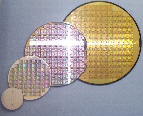
Silicon wafers contain enormous numbers of microprocessors. For example, a typical 300 mm wafer, as used by Intel, can contain about 130 dies of Intel Core i7 “Sandy Bridge-E” CPUs (use the formula, Luke, and substitute S=435 mm² for a die size).

Silicon wafers can contain lots of chips! Image by: Wikipedia user “Stahlkocher”. Source: Wikimedia Commons.
However, after packaging, CPUs take slightly more physical space. And then, density is dramatically lost again when you put CPUs onto a motherboard, and finally enclose that into a computer case. What used to be a thin silicon device measuring just 21×21 mm, now received a huge outer “package”. Of course, a motherboard conveniently integrates other important components such as memory modules and an interconnection network adaptor. But could we manage without integrated circuit packaging in the first place?
Seems that semiconductor engineers from Moscow, Russia have some bright ideas for us.
What they propose somewhat resembles wafer-scale integration, a technology that dates back to 1970s. Its purpose was to build an integrated circuit as big as technologically possible, perhaps the size of an entire wafer.
Now, think of 130 CPU dies on a single modern wafer, and multiply this by, say, 6 cores on a die. Seems like an easy way to build a 780-core system? Unfortunately, things are not that simple.
Wikipedia says that many great companies invested time and effort into wafer-scale integration, and all failed (including a company run by the famous Gene Amdahl, and this fact once again teaches us not to be afraid of difficulties).
One of the problems was a low yield — that is, too many areas of a big integrated circuit contained defects, which rendered the entire big circuit useless. However, if your hardware contains mainly identical elements, such as cores and cache memories, then, even if some elements are later found to be defective, there will still be enough working elements to consider the wafer usable. Connect them after testing, and you are done: one wafer will have 700 cores, another will have 720.
But we still need to provide data for this computing monster to crunch — and then get the results out. Do we need a traditional package with lots of pins? No. That’s where the Russian idea comes in.
Eugene S. Nazarov of JSC Moscow Radioelectronic Plant “Temp” suggests the following:
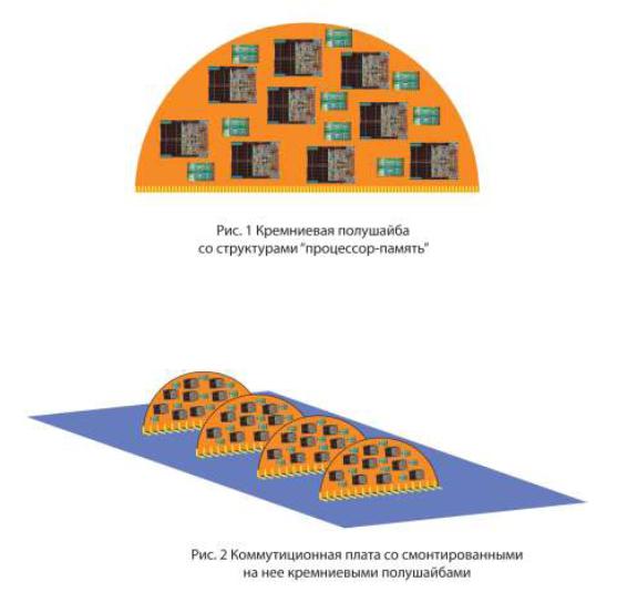
1. Place interlacing sequences of CPUs and memories onto halves of a wafer (half-disks).
2. Test and mark defective elements.
3. Lay down connections between working elements, using usual semiconductor manufacturing techniques.
4. Solder half-wafers, vertically or horizontally, to a switching back plane. (That’s how data will get into and out of the CPU). The back plane must be made of a material whose thermal expansion coefficient is close to that of silicon; copper-plated invar is proposed.
5. Passive electronic components can be SMD-mounted right onto a silicon wafer.
6. The whole system-on-wafer (SoW) is protected with a parylene or similar coating. Since the coating is hydrophobic, the assembly can be easily cooled with water. (That’s something like! I am delighted!)
I will give you a picture from the article to whet your appetite, but to learn more details, you will need to fetch the original PDF file and be able to read some Russian! (Or simply use the Google-Translated version)

From: Eugene S. Nazarov, “Feasibility of manufacturing of supercomputers using system-on-wafer technology”, 2011. Captions: “Fig. 1: Silicon half-wafer with CPU-memory structures. Fig. 2: Switching back plane with mounted half-wafers”
The original article by Eugene S. Nazarov was presented exactly one year ago, on 26 October 2011, at the Moscow Supercomputer Forum.
The website of the Moscow Radioelectronic Plant “Temp” contains more interesting material on their so-called “internal mounting technology”, which is explained to be cheaper, denser, more EMI-resistant and more reliable than corresponding surface-mounting technology widely used today. But, as I am not an expert in semiconductor fabrication, I leave that to the interested readers.
