The idea of using graphics hardware to perform computations dates back to 1978. However, AMD claims that it was them who “kicked off the GPGPU revolution” in November 2006. What is really important is that it was standardisation that allowed mass participation in this movement. NVIDIA’s API for GPGPU, called CUDA, was made available on February 2007, and is currently the de-facto standard.
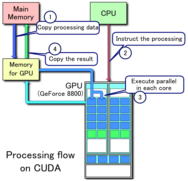
The problems with practical use of GPU computing are two-fold. First, you have to learn the corresponding API — CUDA or OpenCL, or at least bindings for your programming language: see bindings for CUDA and for OpenCL. Second, you have to deal with memory transfers: every piece of data that you want to process must be transferred to GPU memory, and after processing, the result must be transferred back to your regular (CPU) memory:

Processing flow on CUDA that can soon be made obsolete.
Image by Wikipedia user Tosaka. Source: Wikimedia Commons.
These transfers are tiresome to program, distracting software developers from their main task — making their software parallel. But transfers can soon be made obsolete, thanks to the technology proposed by AMD.
The technology is called Heterogeneous Uniform Memory Access, or “hUMA”; read more in this article by Tom’s Hardware. The main idea is that CPU and GPU units have access to the same memory, so everything you load into memory is immediately visible to GPU. This means you no longer need to program data transfers.
As there is only one single memory, no transfers at all are needed. There are other technical difficulties instead, such as cache coherency, but these will be handled by hardware. So, the programmer’s time is freed, which boosts productivity.
Additionally, in current solutions the need to maintain two separate memories and move data between them results in energy inefficiencies: first, DRAM memory consumes energy even if no data transfers are in progress, and there are two separate memories that must be constantly powered on — CPU and GPU memories, while in the proposed architecture there will be only one. Second, moving data between memories also requires energy. Hence having one memory with a uniform access from a programmer’s viewpoint is a good thing. Effects of improved energy efficiency will be somewhat reduced because cache logic that maintains hardware cache coherency will require some power to operate, but simplicity of use will outweigh any of these effects.
The only “hindrance” (if we can call it a hindrance) is that the proposed solution is static (non-modular). With current solutions, where CPU and GPU each have their own memories, you can plug one or many GPU accelerators into a uniprocessor or a multiprocessor server — that is, you have flexibility as to how many CPUs and GPUs you have in a server. You can have almost any combination; the only requirement is that your software can utilise the hardware resources efficiently. And you can always rearrange components in your servers to move to different configurations.
With the proposed hUMA architecture this flexibility is reduced. From the technological point of view, it is the most convenient for the manufacturer to put a fixed, unchangeable number of CPU and GPU engines onto a single silicon die (AMD proposes just that), and these will communicate to memory modules located on the same board (usually soldered). You can’t just add more CPU or GPU engines or more memory to this system to make it more powerful — you need to add a second system instead.
This way, a single hUMA system will be good for mobile computers (notebooks and tablets); in this market segment the word “upgrade” usually means buying a new device. Multiple hUMA systems, interconnected with a fast network, will be good for parallel computing.
One last thing to note: once we start using hUMA, it will be difficult to go back. Software written for hUMA architecture will not know how to use traditional GPU accelerators, because it would have lost the very notion of manually programmed data transfers between CPU and GPU memories. But maybe it’s time to say goodbye to those manual data movements.
